We Provide
AI Powered 2D/3D inspection software/Hardware Solution for Semiconductor Manufacturing
Solving our clients’ toughest challenges through our advanced machine vision technology.

Work with INFUSE3D
We commit. We deliver.
We are a company where cutting-edge technology converges with a commitment to revolutionize the landscape of semiconductor manufacturing. As a high-tech company, INFUSE3D is at the forefront of innovation, specializing in the research and development of sophisticated machine vision and software solutions tailored for the semiconductor industry.
At INFUSE3D, we recognize the critical role that advanced vision technology plays in empowering high-end manufacturing processes, particularly in the realm of integrated circuits. Our primary focus lies in creating groundbreaking solutions that enhance efficiency, accuracy, and quality within semiconductor manufacturing.
Key highlights of our offerings include state-of-the-art 2D and 3D sensors designed specifically for semiconductor defect detection and measurement. These sensors serve as indispensable tools in identifying and analyzing imperfections, ensuring the production of flawless semiconductor components. Additionally, our products extend to semiconductor process quality analysis, providing comprehensive insights that drive continuous improvement in manufacturing processes.
In addition to our cutting-edge hardware solutions, INFUSE3D takes pride in offering robust software solutions tailored for semiconductor equipment and various other industries. These software solutions are meticulously crafted to optimize operations, enhance productivity, and streamline workflows, contributing to overall operational excellence.

Application and values
With our continuous innovation in inspection technologies, algorithms, and processing capabilities and high-speed, high-resolution 3D sensors combined with AI-powered software that we‘re developing, we provide a transformative solution to below challenges of IC packaging, Advanced packaging, Memory/SSD module inspection/measurement.
High Resolution and Accuracy Requirements
Complex Geometries
Surface Reflectivity
Defect Types
Throughput
Data Processing
False Positives/Negatives
Technological Evolution

> IC packaging inspection
Our solution designed to seamlessly integrate into IC packaging inspection machines, enhancing yield and efficiency in production environments. Our advanced inspection capabilities ensure that each IC package meets stringent quality standards by accurately measuring key parameters and detecting various defects. By incorporating our technology into your production, you can achieve higher yields, reduced waste, and increased customer satisfaction.
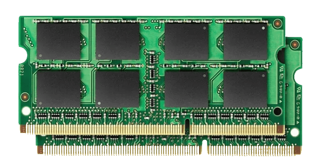
> Memory/SSD module inspection
Enhance accuracy and throughput in Memory/SSD module inspections by integrating Infuse3d software and hardware solution. we leverage advanced technology for high-precision, high-throughput production environments and fulfils memory/SSD module post-test and pre-shipping inspection requirements.
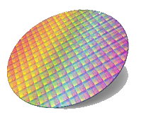
> Advance Packaging wafer level Inspection and Metrology
Integrating our technology into wafer inspection machine enhances its capability to deliver a comprehensive range of wafer inspection and metrology solutions, ensuring the reliability and precision needed for future generations of stacked devices.
.png)